
We have been celebrating the coming double boost to the semiconductor sector: A recovery from the worst cyclical slump in 30 years and a secular boom arising from “computation everywhere,” as the microchip increasingly moves out of safe environments and permeates the world. Kulicke and Soffa Industries (KLIC) goes one better, explains George Gilder, editor of Gilder’s Technology Report.
It gets yet another boost from a powerful shift in revenues and margins within the semiconductor industry. Chip packaging and assembly, once minimally profitable segments, are becoming major sources of value added.
Packaging and assembly become crucial as heterogenous elements of a system. Once contained on separate chips or awkwardly fabbed together on processes suboptimal for one or the other, they are now increasingly joined together in the packaging itself. Along with systems on a chip (SoC), we now have systems in a package (SiP).
KLIC is a leader in developing and manufacturing equipment, tools, and materials used in chip packaging and assembly. Packaging is giving us better, faster, cheaper—and especially—smaller devices. Smaller has been a relentless goal of the industry forever: Devices made of vacuum tubes cannot pervade the world. And smaller usually means cheaper—more chips per wafer—and faster, because signals traverse shorter distances, and therefore with less power.
At KLIC, the drive to get real small has deep roots. The company first came to our attention for its work in LED display technologies—a field also driven by the quest for diminishing dimensions. More good news about that below, but first let’s talk about artificial intelligence (AI).
Advanced packaging is also a crucial enabler of data-addicted AI hardware. It’s the packagers who enable the chip designers to combine different types of processors and memory in innovative configurations, getting the data to the processor and back faster.
Supporting these configurations are multiple, innovative interconnect technologies, used to connect die to their substrates and to one another in multi-chip packages. The interconnect technology determines how the chips are stacked and bonded in a package. As devices continue to shrink in size and increase in complexity, such mechanical aspects rise to the fore.
Another advance for which K&S has taken a strategic leadership role is the “vertical fan-out” (VFO) approach. Here’s what it looks like:
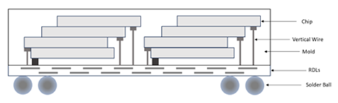
In VFO packaging, the die within a stack of chips can be offset to accommodate the vertical wiring, rather than have the wires run through holes in the chips as used by a 3D packaging technology called through-silicon-vias (TSVs). VFO uses the space created by the offset to route these connections around the silicon.
All told, K&S is a leader in new these exciting new forms of packaging technology; packaging, increasingly, is where the money is.
Recommended Action: Buy KLIC.